






Ever wondered what the future of microprocessing looks like? From Photonics to Death-Rays, explore the possibilities.
Silicon, due to its semi-conductor properties is currently the best known material for microprocessing units. Several Silicon/metal or oxide compounds are used for various effects on current CPUs to alter resistence or conductivity. So how can we improve performance of silicon processors? Well many will know the answer to that and that is down to one of two things.
• The architectural design
• The fabrication process
The architectural design is not something we will touch on as that is a variable that can change at any level, however the fabrication is the playing field, it is what denotes the physical limitation of the CPU die. The smaller the fabrication of transistors, the more transistors you can fit into the same die space. Current fabrication in use by Intel is the 32nm (nano metre) node. This shrinking process follows Moore’s Law though there is a limit to that too and that is the atomic level of the material itself. Working at such a fine resolution causes issues too, such as impurities in the material or dust contamination.
Thus the smaller the fabrication the more sensitive the measures needed to be taken to reduce/limit contamination and the more sensitive the manufacturing procedure of silicon wafers to reduce impurities and inconsistencies. Current lithography techniques are very refined to reach the current resolutions and procedures tend to mature as the finer processes become more common.
Lithography Types 1
Current Lithography
The current mainstream fabrication uses what is called Immersion Lithography.
Just 2 years ago it was expected that sub 20nm would arrive around 2016 but with Moore’s Law remaining true Intel will be shipping 22nm chips in 2012 with 14nm to arrive 2013 and 10nm in 2015. Current 32-22nm resolutions are made using multiple patterning. Double patterning has been in use for a while and triple-multiple patterning will be used for sub 22nm.
Multiple patterning has its limits though, even if it can whittle down to sub 10nm, unless the litho technology improves along with the resolution it may no longer be realistically usable due to poor focal tolerences (printing over the same spot?) or poor output (wafers per hour).
EUV lithography
Extreme UltraViolet lithography was originally hailed to be the successor of current mainstream lithographic processes with a theoretical resolution down to 2nm. As with anything new, it is very expensive and requires a lot of power to create chips that are comparable to current fabrications. Though experiments continue with EUV there are more and more hurdles that keep arising such as the polarising nature of EUV radiation as well as requiring even MORE power for multi patterning as well as requiring complex multilayer optics and expensive superconductive magnets to control the scatter and definition. Intel had hoped to start using EUVL for its <10nm fabrication but the technology is behind in its development and is proving too costly. While the physical potential is there, the technological hurdles and resources required for it to be usable, simply, is not feasible in the near future and likely will not be in mainstream use for maybe another 10 years.
Lithography Types 2
Other Lithography Techniques
There are various forms of photolithography each with different strengths and weaknesses though not all are suitable for printing semi-conductors.
Includes:
• Electron beam litho (e-beam litho or EBL)
• Nano-imprint Litho (NIL)
• Ion bean Litho
Electron beam lithography is a very fine and high resolution process but is known to have a slow throughput and because electrons have a physically ‘near non existent’ mass thus the ‘photoresist’ requires longer exposure to the lightweight beam. Although the primary e-beam has a fine resolution it suffers from ‘scattering’ of secondary electrons which causes imperfections in the photo resist. Limitations to around 20nm are best in regards to quality as secondary electrons have been observed to travel over 100nm. Back scattering is an issue too, this is when electrons from the primary beam bounce back and disturb the beam whence it came.
Intel are using e-beam lithography on their 22nm Ivy Bridge CPUs to create the 3D ‘Tri-Gates’ and as e-beam processes mature, patterning of 5-7nm has been verified as methods to control scattering develop.
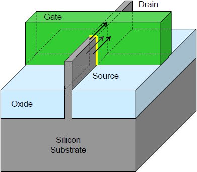
Intel’s 3D ‘Tri-Gate’
Nano-imprint lithography is a novel and relatively simple technique using fine templates which can be whole wafers or individual dies. It is also relatively simple to create ‘3D’ patterning as it simply neds to be etched into the template. However this process is limited to the abilities of other lithographic processes to create the templates and the templates suffer from wear as with any mechanical device. Despite its advantages it is not considered to be an ideal option.
Death-RAY
DEATH RAY
Ion-Beam Lithography and 3D fin-FETS
Ion beam lithography is separated into 3 types:
• FIB (Focused Ion Beam),
• Proton Beam Writing (p-beam writing)
• Ion Projection Lithography (IPL)
Ion beam lithography allows carving and shaping of silicon and is able to create 3D architectures. I am sure that it will eventually play a major role in semi conductor fabrication and here is why.
Ion beam lithography uses protons rather than electrons, while electrons may have a theoretical higher resolution, we are dealing with elements and these elements are made of atoms thus sub-atomic leptons, that is, electrons, are not an ideal solution to be displacing the comapartively gargantuan atoms.
Using Neon or Helium ion beam lithography (NIBL, HIBL)has been reported to be ~ x1000 times more efficient than using EBL at resolutions of 5-7nm. Helium of course is the second smallest atom thus with refinement maybe it is possible to edge it up to terminal resolution.
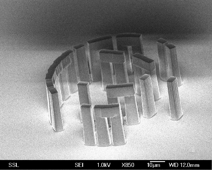
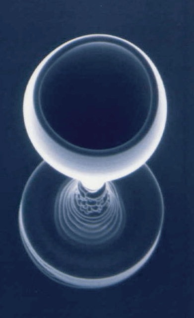
The above images show how ion beams can create 3D shapes
As with almost everything to do with physics, physical surface area plays a hugely important role in the conduction of practically everything from heat to electrical current and to overcome the physical limitations of 2D architecture, soon we will be entering a phase of 3D microarchitecture with Intel’s 3D ‘Tri-Gates’.
I would like to point out that this is not an Intel innovation but they will be first to implement the technology in mainstream production. Most other semi-conductor companies argue that fin-FET or multi gate transistors are not needed until sub 20nm. Now, just an explanation, 3D transistors does NOT = 3D architecture. In fact it is often referred to as 2.5D or two and a half D this is because interconnections on the CPU are ‘still’ planar. The process of using ‘3D’ multi gate transistors or fin-FETs using either e-beam lithography or Ion-Beam lithography will eventually become commonplace.
I’m not overly interested is discussing how transistors work but to briefly skip on some details (I’m not expert so forgive me for any inaccuracies). Transistors switch on and off, this is the I/O signal or your digital 1s and 0s, the faster they are able to switch on and off (frequency in Hz/MHz/GHz etc) the more signals they can send and the faster they can move data (depends on architecture design too) but as fabrication gets smaller, electrical leakage becomes an issue. Leakage reduces CPU power efficiency and as you increase transistor frequency/add more volts i.e. potential difference, the more leakage there is and the CPU eventually becomes unstable. Leakage can cause overheating (resistance increase) instabilities in performance (incorrect signals on/off) physical warping (temporary and permanent) of transistors.
To curb leakage
• The materials need to be changed (á la HKMG)
• Temperature needs to be reduced
• Increase conductive on state
• Increase resistive off state
The latter two points are what 3D transistors are able to achieve through the basic surface area principle and it is why lithographic processes need to be able to consider the ability to create ‘3D’ transistors.
Limit to Performance?
What kind of Performance Can We Eventually Expect?
Whilst I’m sure many have heard of the previous experiments of cluster based processing experiments like the 80 core CPU from Intel?
The 80 cores were experimental and are nowhere near as comprehensive as contemporary CPUs, it is likely that these experiments inspired future (current?) and beyond CPU designs. Does this mean that we should expect mega cluster processing units in future?
Say for example, we scale down a 32nm i7 2600K with a die size of 216mm² with 995,000,000 transistors.
@ 2nm in the same die space we could fit in direct translation (its more complicated that direct scale down mind.) approximately 255,000,000,000, which is about 256 times more transistors.
(An issue with this conversion is that the i7 2600k has used about 20-30% of die space on GPU. Due to the architectural differences in GPU and CPU there is likely to be difference in concentrations of CPU transistors and GPU transistors etc. This conversion isn’t meant to be accurate, just to highlight how vast the difference between 32-2nm is.)
Regardless will this mean that we can expect CPUs with hundreds of cores come 2nm fabrication? Or will the implementation of new architecture with larger more complex cores arrive while sticking to <100 cores per die?
By Moore’s law, we are only 5 generations away till 2nm @ 18months per Gen.
• 22nm- 2012-2013
• 14nm- 2013-2015
• 10nm- 2015-2017
• 6nm- 2017-2019
• 2nm- 2020> ?
We are likely only to be around 10 years at most away from 2nm fabrication, technology dependant.
If we assume 15% performance increase per generation +10% per new architecture, can we expect that with 2nm fabrication that we may get a 128 cored CPU with 256 threads that are 160-200% better than Sandy Bridge per core?
I’m sure the scaling and architecture changes will be different from those numbers but it does give basic insight to where we are heading in future. This doesn’t include utilisation of GPU cores, which is definitely going to happen which will bring more performance benefits in highly parallel workloads and floating point calculations. But once we are at 2nm fabrication, performance will only be dictated by die size and microprocessor design.
By moving into 3D space, die size and design potentials can be vastly expanded.
3D Stacking, Photonics and Trans Superscalar Micro Architecture.
Intel not too long ago have started a lot of research into photonics and silicon lasers as an ultra fast data transport using light itself. While early implications of light photonics may be for data storage/transfer, it’s possible that it is something that could eventually be used for on-die interconnects. Intel are experimenting with 1Tbps data speed as copper wire is reaching its physical limits of data transmission.
3D stacking is creating microarchitecture in multiple layers that all interact with one another. REAL 3D architecture is literally this, stack upon stack of dies interconnected. This seems to be a more crude construction of my thought of completely interconnected designed and manipulated 3D crystal but I give myself too much credit there.*(See final chapter)
Recent article about IBM and 3D stacking.

Diagram showing how a 3D CPU ‘Brick’ is stacked in layers.
Eventually this technology will lead to a Trans Superscalar MicroArchitecture, which is a term I made up to describe the next level of 3D silicon Microarchitecture. By using 3D stacking, CPU cores will eventually be able to communicate not just along the X and Y axis but also up and down the Z axis creating new pipelines and bandwidths fuelling greater CPU performance. It would even be possible to have layers of pure cache sandwiched between layers of pure x86 cores and a layer of media functionality and graphics.
IBM predicts that this method could be x1000 more powerful than current processing solutions, now combine that with a cost effective 2nm fabrication process. The result could simply be pretty immense.
Issues with 3D Stacking?
One of the primary concerns and hindrance of 3D stacking is ‘thermal density’. Creating such a dense block that develops heat through every layer can cause serious issues. So what about cooling? With IBM and 3M’s announcement about the thermal adhesive, it is definitely progress in heat dissipation but in a solid brick of processing grunt, will thermally conductive layers help? Will the shape of the stacked CPU ‘brick’ need to change for cooling purposes? Will new types of coolers be able to suffice? Or will the future see the need for these 3D cores to be suspended in coolant?
Platform design will need to be considered too. The more that happens within the CPU, the more highways you need to get the data out and then we need to talk about the physical limitations of PCBs. No doubt that once we start talking of 3D architecture, would it not be wise to assume that supporting interfaces will also need to be in a three dimensional manner too?
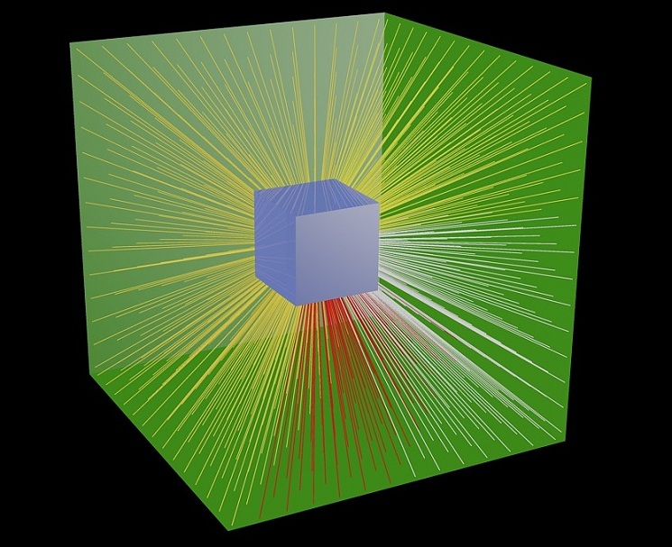
Possible Example of how a Complete Trans Superscalar Microarchitecture CPU core may look?
So What Will Happen Next?
There are physical limitations that need to be considered with all the materials we use on an atomic level. Either we need to find an element with smaller atoms with similar properties to silicon. Or create some novel materials.
The only other element worth replacing silicon with is Carbon. Carbon however is a very complex element in its molecular possibilities. As Graphene, its use is not suitable for CPUs. This doesn’t rule carbon out completely. It may just be required to find the correct molecular structure that provides the necessary properties. My prediction is that it will be somewhere in between carbon nano-tubes and crystal diamond, however for this to be possible, atomic manipulation of carbon is needed in an atom by atom construction. Will this even work? Or will it even be possible? One day maybe but at a guess it will be complicated and I expect it will require direct real time manipulation of carbon bonds jumping between sp2 and sp3. Diamond is an excellent electrical insulator while carbon nano tubes in multi-layers are potentially natural super conductors. Though the molecular geometry involved, if possible, blows my mind even trying to think of such thing.
Then again maybe I’ve watched far too many Sci-Fi movies.
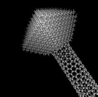
The above diagram is a display of how carbon nano tubes can interact with diamond on a molecular level.
While researching into my idea, I came across this video.
Of course there is the possibility of Quantum computing or Biocomputing that will eventually mature along with nanotechnology. My guess would be that it is a matter of which is most feasible and cost effective at the time of application. Still I like my idea of having completely artificially constructed diamonds suspended by nano tubes and lasers with molecular bonds that swap between uber electrical resistor to super conductor… such a pretty thought.
Wonder if they could do them in pink?


